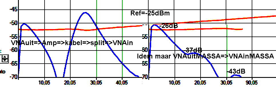
Test signal connected in respect to ground in parallel to both antenna inputs.
Result after making four solder connections : Difference at 25MHz abt. 25dB !!
Before After
| << |
NanoVNA modification |
In the "Tiny Vector Network Analyzer"
nanoVNA, the transmitter part and receiver part get power from the same source.
However, the grounding contacts of the output-SMA-bus "TX" and input-SMA-bus
"RX" are not directly interconnected.
While
measuring with the nanoVNA :
- delivers SMA bus "TX" a test signal to the device under test (DUT)
- is the output of that amplifier under test connected to the nanoVNA
input-SMA-bus "RX" and
- compares the nanoVNA the difference in RF voltage and phase between SMA
busses "TX" and "RX".
It therefore is important to keep the electrical path between "TX" and "RX" as short as possible to keep time delay and phase difference minimal. If some RF current runs in the ground connection between "TX" en "RX, it will generate RF voltages, disturbing the accuracy of the measurement. Especially when measuring high gain equipment.
Measuring the frequency characteristic of a high gain DUT, for instance the antenna amplifier "pa0nhc Small Active RX Loop", some voltage difference can occur between the DUT's input and output. This will result on the outside of the screening of the coax cable in a small parasitic RF Common Mode Current between DUT and nanoVNA "RX". The amplitude and phase of which will vary with frequency.
Strange phenomena.
Measuring "common mode suppression"
of my active RF loop amplifier, the results were disappointing.
Jittering the BNC plug connections seem sometimes of influence.
When (using a screw driver) directly connecting the ground surfaces of the RX-SMA
ad TX-SMA together, the plot of the frequency characteristic changed.
Cause :
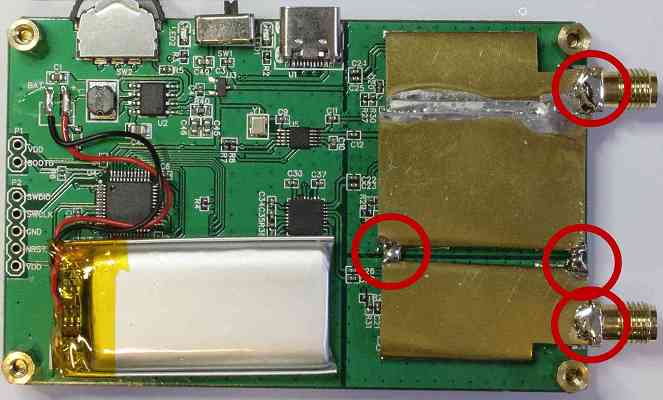
The nanoVNA has no direct connection between
"RX" ground and "TX" ground.
- The TX and RX ground surfaces are separated by isolation tracks.
- The brass screening foil of the TX part and RX parts are not connected
together to interconnect the RX and TX ground surfaces.
- The brass screening foil of the TX part and RX parts are not connected
to their SMA bus ground.
Small RF currents running between "RX" ground and "TX" ground, will generate RF voltages and phase differences between "RX" and "TX", which can disturb the graphs of measurements.
Solution :
After soldering four points, the path between
"RX" and "TX" was short and wide, and the impedance of
the ground path minimal. Measurements are more stable, more reliable, and more fulfilling expectations.
See pictures below.
TIP : In order to reduce possible spurious RF currents to a minimum, on the connecting cable between DUT-output and nanoVNA "RX"-input a Commn Mode Choke was installed. It contained 4 turns RG58 into a 29mm FairRite #31 ferrite "SnapIt" core. Exactly like the loop antenna is connected to its splitter in practice.
Common mode suppression
measurements onto a balanced high gain broadband RF amplifier.
Test signal connected in respect to ground in parallel to both antenna inputs.
Result after making four solder connections : Difference at 25MHz abt. 25dB
!!
Before
After
How to :
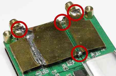
Remove the bottom plate of the nanoVNA.
Use a thick solder point at 360 C.
See photo's.
- Solder the RX-SMA flange to its brass screening foil.
- Solder the TX-SMA flange to its brass screening foil.
- On two points interconnect both screening foils by soldering the
screening foils to each other.
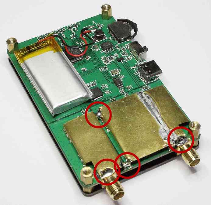
Reinstall the bottom plate.
Recalibrate the nanoVNA.
Success, Nico pa0nhc.
|
||
|