 |
 |
| << |
Pure Signal Power Tap V2 for the Hermes Lite2.
|
|
|
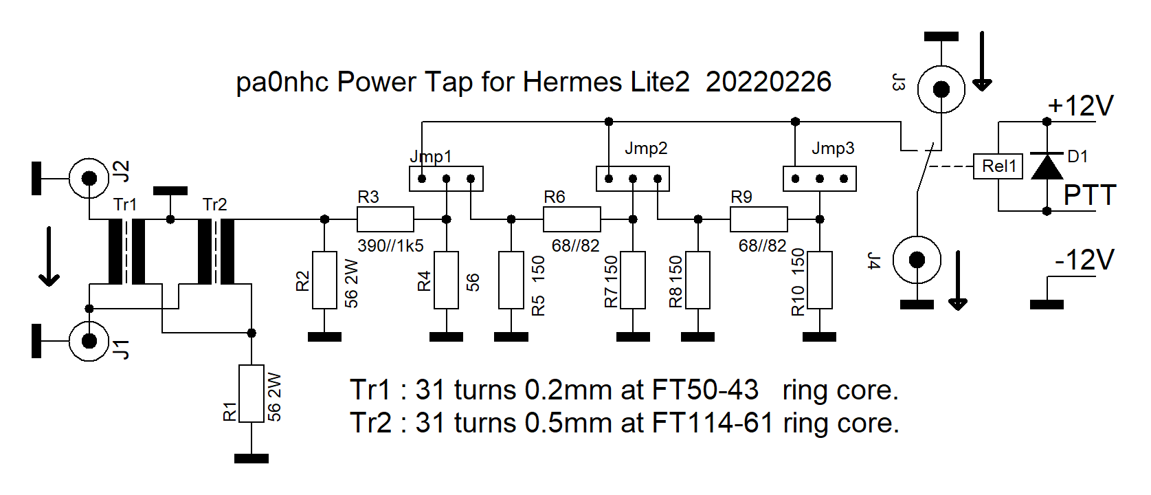
Schematic.
The 31:1 coupler (Tr1,Tr2,R1,R2) is copied from a design by DC6NY.
It is connected to a 3-stage
(22dB+6dB+6dB) 50 Ohms attenuator (R3-R10). As the max. input level of
the HL2 is just above 0dBm, the attenuator outputs are rated each to be somewhat
lower.
If an output power correction at J4 is needed, the value of R3 can be adapted.
Connections J1, J2, J3 and J4 are 50 Ohms with low VSWR.
PCB.
The shown PCB is will become available as soon as
enough HL2 users are interested in it.
The PCB designed for good RF properties. Top and bottom ground surfaces are inter connected by multiple via's. 50 Ohms lines are 107mil wide wherever possible. The grounding pins of the SMA busses can be soldered onto both top and bottom grounding planes. The relay is Fujitsu FTR-B3SA 12V with double contacts in parallel. To prevent the influence of eddy currents in the top copper surface under Tr2, the PCB top copper layer is there removed. I advise to keep at least 5mm extra distance between the PCB top surface and Tr2 bottom. Use some extra insulation.
Housing, drilling.
The PCB is designed to fit inside a Hammond box 1590C. The position of all holes
should be so, that after installing the PCB with the SMA busses screwed tightly into their SMA
holes, the PCB upper surface just touches the underside of the N bus pins,
without bending the PCB. Keep in mind, that
the sides of the box are tilted for a few degrees. To prevent bending of the PCB
lateron, the holes for the SMA busses should best be drilled a bit lower than
those for the N-busses.
FIRST drill the
holes for both SMA output busses and the relay bus in the opposite side of the
box.
Then temporarily mount the PCB firmly into the SMA holes.
Mark at the opposite box side the horizontal center line for the N-busses (top
of PCB surface).
Mark the centers of the N-connectors (centers of PCB tracks).
Remove the PCB.
Copy the N-bus center lines to the outside of the box.
Draw the position of all holes.
The four little screw holes for each N-bus should be drlled 2,4mm and tapped
M3.
At the inside only one nut is then needed for the ground lug. This
simplifies the N-bus and PCB installation.
Then drill and tap all the holes for both N-type busses.
Installing.
Install the PCB with the SMA busses into a box side.
Use the original tooth rings between
the nuts and the outside of the box.
After that : install the N-busses with four M3 screws.
At the PCB top corners near the N-busses are two solder able grounding surfaces.
Grounding lugs at the N-busses must be directed to become in contact with such a
surface.
Install a grounding
lug at one screw of each N-bus, with a tooth ring and a nut.
If the box is painted, remove the paint under
the tooth rings first.
Solder the
N-bus ground lugs to the PCB corners.
Solder the N-bus center pins onto the PCB tracks.
Important :
All "ground" contacts of the N- busses "IN" and
"OUT", AND of the tooth rings under the nuts of the SMA
busses, shouldl make good electrical contact with
the OUTside of the METAL box. Remove outside paint if
necessary, using a steel brush and a drill.
Remove also paint under the tooth rings for the inside grounding lugs at
the N-busses.
Checking.
Put the three jumpers in their appropriate positions as follows :
- First put all three jumpers in positions marked
with "-" .
- After that, change one jumper to position "???W",
to set the J4
RF output in
accordance to the maximal input at "IN".
As an example : for 300W max amplifier output set jumper to "400W".
Connect a power amplifier and a high power dummy load to
"IN" and "OUT".
Connect a small 50 Ohms dummy load to J3.
Connect an RF oscilloscope with added 50 Ohms load, or a 50 Ohms RF dBm meter (0
dBm range) to J4.
Connect 12V between "+12V" and "PTT".
Apply for a few seconds maximal 3.65MHz RF power, and check that the RF output
at J4 does not be higher than 200mVrms.
If an output power correction at J4 is needed, then change the value of R3.
TIP : R1 and R2 will become HOT at high power.