 |
 |
|
Analog automatic tuner for a “Magnetic" loop antenna. pa0nhc 20160321 / 20180204 / 20220125
|
This is a modified and upgraded version of the
PE0RIG design, published in Electron October 2014 page 430.
It is optimized for use between 3.5 and 7.2MHz.
The here described design is for use near the transceiver.
A version connected directly to the antenna is possible, but not
described here.
If used on higher bands, i advise to reduce the number of turns on L1, and adapt C17 and C201.
My automatic loop tuner was connected to the 10m circumference loop, using 27m 50 Ohms coax cable, and a 5-wire motor drive cable.
For good performance, the current sensor and phase detector PCBs are now separated.
The four TO220 driver transistors are mounted on the bottom of the cabinet.
PDF
downloads:
Print
the drilling templates in "100% size" or "Original size".
| Partslist | Schematic | Layout | Parts locations |
Drilling template Proma cabinet |
Drilling template front (parts locations) |
Drilling template back (parts locations) |
A
printed A4 construction manual can be ordered. Price 12,50 Euro.
How does it work?
Important: For a stable operation, the RF voltages on inputs "CAR" and "SIG" MUST have amplitudes between 300mVpp and
1400mVpp.
The voltage on "CAR" is IN phase with the voltage on the transmission line.
Suppose phase detector IC1 gets on inputs "CAR" and "SIG" two voltages of the same frequency, but with 90deg. phase difference. IC1 then generates on both outputs ("OUT" and "OUT' ") square wave HF currents, each with exactly 50% duty cycle. After filtering, their effective voltages are then exactly equal. There is no voltage difference between both outputs .
Current sensor L1 transforms a part of the RF current in the transmission line, into a HF voltage. The secondary winding of L1 (1uH) is nearly UNloaded. Resulting in a phase shift of nearly 90deg. between antenna input current and output voltage of L1.
In the feed point of a correctly tuned antenna, both HF current and RF voltage have the same frequency, and are IN phase (0deg. phase difference). The voltages on "SIG" and "CAR" then will have a phase difference of 90 deg. Resulting in equal DC voltages on "OUT" and "Out' " (abt. 7.8V). REM: the fairly large HF components are filtered out by C15 and C16.
As no voltage difference exits between both outputs of IC1, motor lines [M1] and [M2] do not contain any drive voltage for the motor, which stands still. Without RF signal on the antenna feed line, the motor also does not run.
When the antenna is not correctly tuned, the RF current and voltage on the transmission line are OUT of phase. The voltages on "SIG" and "CAR" now do NOT have exactly 90deg phase difference.
The result is that the DC voltages on "OUT" and "OUT' " change in OPPOSITE directions. Consequently
there is a voltage difference between M1 and M2. The tune motor now runs, until it re-tuned the antenna and the phase difference between both inputs is exactly 90deg.
again.
|
|
Modifications to the original PE0RIG
design :
The tuner is installed in a little, screening ALU (eurocard) Proma cabinet, together with a noise-free 12V 0.85A power supply, which also
feeds both relays and the anti-condensation heather in the antenna box.
IC1 is fed by a 9v stabilizer. The values of R5, 6 and 7 are accordingly adapted.
R15 prevents static build-up on C4, should the antenna not be grounded for DC.
C2 is enlarged for better decoupling. C3 and R9 also are adapted.
C15 and C16 prevent the (fairly strong) RF currents reaching IC2.
Current sensor L1 and the current shunt have changed dimensions. L1 can be wound on a Amidon T50-2 or T50-6 iron powder core (D=12.5mm, u = 8 to 10, L (not critical)=0.4uH ).
During operation on the 3.5MHz band, Rel1 on the current sensor board adds a small capacitor
C201 in parallel to C4/C17. This compensates for a small difference in set point of C4, when switching down from the 7MHz to the 3.5MHz band.
REM: Rel1 switches together with a impedance matching relay in the tuner box (see "Efficient "MAG" loop transmitting antenna") .
>> D3-6 limit the HF voltages on IC1 inputs to abt. 1400mVpp, to prevent instability of IC1 outputs, due to overdrive <<
T1-4 showed to form a HF/LF oscillator, together with the self inductance of the motor. C12, 13, 14 and R9 suppresses this unwanted phenomena.
Details of the current sensor.
The primary of L1 is a (1.7mm dia) link, going once through the hole of the Amidon T50-2 or T50-6 powder iron ring core.
The secondary winding (0.5mm dia insulated wire), is going 10 times through the hole in the ring core.
REM: the winding direction determents the phase relation between "SIG' and "CAR". If ANT and TX connectors seem to be reversed, rewind L1 with the secondary in
opposite direction.
A HF-SHUNT runs around the core (not through the hole). It bypasses a part of the current in the transmission line, AND lowers the (otherwise to high in the line inserted) impedance of the primary of L1.
In the prototype the shunt was a piece of wire 0.7mm dia and abt. 40mm long, shaped in a U form. It is soldered DIRECTLY onto the connection points of the link (onto the primary of L1 which runs through the ring core). See photo.
REM: for use on higher frequency bands, adapt L1, C17 and C201.
Cooling.
At 0.6V motor supply voltage, the motor starts and stops running. When the antenna is tuned, the motor supply voltage still could be 0.6V,
and the motor current 0.5A. Two of the driver transistors T1-4 then have to dissipate continuously 2x 3.5W. They are therefore cooled by screwing them (the PNP's insulated) onto
the bottom of the ALU housing.
As soon as the antenna is tuned, the tuner can be switched-off by switching the 12V power, not the primary 230~AC. Both relays and especially the anti condensation heather in the antenna box should always have 12V supply.
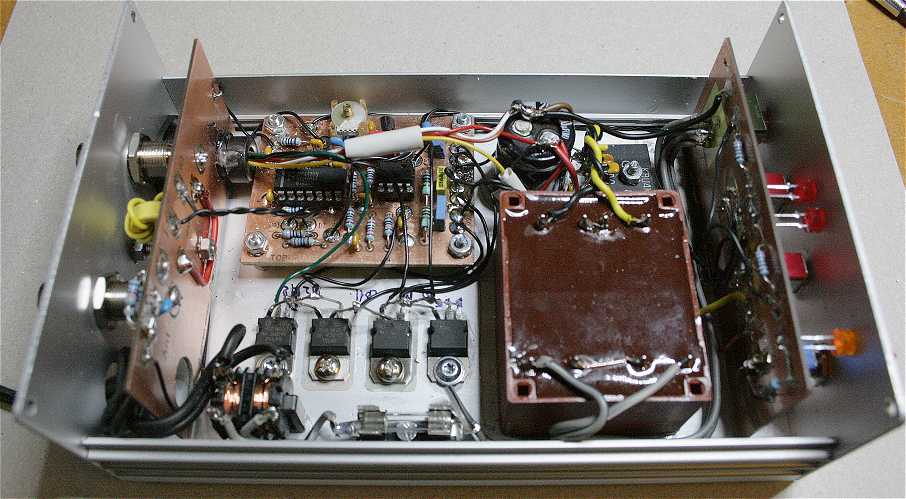
Prototype. REM: the current sensor PCB layout is changed and contains a relay.
The I / Io wires between both PCBs should not be twisted.
The mains voltage is always connected to the transformer.
The on/off switch on the front now switches the +12V line to the phase detector PCB.
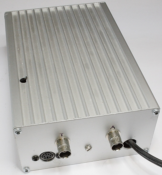
The current sensor is situated on a double sided PCB, which is mounted onto an M3 grounding screw and the BNC receptacles in the ALU back panel of the housing. Except the relay, all components are situated in-between the back panel and the PCB. The antenna and current sensor circuits are screened this way from the tuner PCB.
IMPORTANT: for optimal performance, the wire on "I" should have low stray capacitance. Keep it free from surroundings.
The motor power cable is connected to back plane of the tuner with a 6 pole mini-DIN connector.
The cable wires are:
Two motor wires (orange and green, pins 3 and 4 <=> pcb {M1} and { M2} ).
One band switch relay wire (brown, pin 5).
One +12V anti condensation heather wire (blue, pin 6).
Four "ground" (-12V) wires in parallel (4x white, pins 1 and 2).
A high-Mu ferrite core in the cabinet, shifted over the wire bundle behind the mini-DIN receptacle, blocks RF.
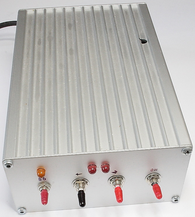
On the front of the cabinet are:
One on/off switch, switching the +12V power to the phase detector PCB..
One band switch with yellow LED, indicating 3.5MHz operation, switching Rl1 on the current sensor board, and the matching relay in the antenna box.
And two push buttons each with a red motor LED, forcing the motor to run fast in a direction of choice.
The two red motor LEDs indicate the voltage on both motor wires in respect to mass. If both are glowing equal, the tuner is on, the motor stands still and the antenna is tuned. If one darkens, the motor runs fast. If both are dark, the tuner is switched-off.
The two sets of 5 diodes function as a threshold, making the difference in brightness of the red LEDs more obvious.
Power.
A simple, but adequate and noise free internal power supply also can deliver the current for the 4.5W anti-condensation heather in the antenna box.
A choke blocks RF in the mains cable. A 100mA slow fuse protects the transfomer against overload. Four C's on the bridge rectifier prevent rattle and IMD. The flat-type
transformer, the elco and the mains choke are glued upside-down onto the bottom of the cabinet. I used Pattex 100% active glue (water resistant). All other components are screwed
onto the bottom, the NPN transistors insulated. T1-4 and the bridge rectifier with a little cooling paste.
For your convenience i made a drilling template. Observe the horizontal lines, which indicate the MIDDLE of the valleys in the cooling
profile on the bottom of the cabinet. M3 screw heads and nuts will just fit here. REM: file screw ends flat with the nut after screwing them, and stick the four feet onto the
bottom.
Adjustment / setup.
The RF voltages presented to inputs "SIG" and "CAR" of IC1 MUST be minimal 300mVpp
and maximal 1400mVpp.
Only then a stable operation of the tuner, and adjustment of C4 is possible.
On 3.5 MHz the output voltage of L1 must be adjusted ONCE, by changing the length of the shunt wire parallel to the primary of L1. A longer shunt wire means more output and vice-versa. See photo and back PCB XRAY.
1. On 7.1 MHz feed 5W into a dummy load. This should generate 800mVpp on input "I", measured with a oscilloscope.
2. Drill a 6.5mm trimming hole above C4 in te top of the cabinet, and close the cabinet.
3. On 7.1 MHZ, feeding 15W into a good dummy load, trimmer C4 should be adjusted for less than +-10 mV DIFFERENCE between both motor wires M1 and M2.
4. Without re-adjusting trimmer C4, on 3.65 MHZ, feeding 25W into a dummy load, the voltage difference between both motor wires should be less than +-10 mV. If this is more, adapt the value of C201 (nominal ca. 10pF).
5. On 7.1 MHz and 3.65 MHz, varying the RF power between 5W and 100W, or transmitting SSB, check that the voltage difference between M1 and M2 will not be more than +- 30mV.