  |
| << |
pa0nhc low noise wide band
VHF pre amplifier. |
|
(C)
The use, copy and modification of all info on this site is only
permitted for non-commercial purposes, |
This little PCB MUST be DOUBLE sided, 1.6mm FR4 Er = 4.35 .
Only the TOP copper surface is shown.
The bottom copper contains NO traces, it is FULL copper and serves as return for
in-out and power.
At strategic places (indicated by "+")., the bottom copper must be
inter connected to the mass planes at the top copper, using rivets or short
pieces of thick wire, soldered on both planes.
Electronic parts are to be soldered on the top copper.
Download the accurately printable
PCB 44 x 25 mm2 PDF for
DIY PCB :
- <right-click> on "PDF"
- click "Save as".
Open the PDF in Adobe Reader and print as 100%.
In- and out traces have a characteristic impedance of 50 Ohms.
As the RF currents should flow
in the shortest routes via the bottom copper surface between IN, T1 and OUT , :
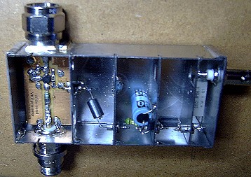
- The top copper mass plane must be soldered DIRECTLY and SHORTLY to the mass surfaces of the connectors
(see "+" and photo).
- The PCB may NOWHERE ELSE come in contact with, or be soldered to the metal box.
Construction.
The PCB is double sided, with the
non etched back plane acting as "ground" surface.
Download the TOP the PDF file, and print it
AS FOLLOWS (commands can vary with printer type) :
- on inkjet foil
- at size 100% or "Original size" (resolution is 200
DPcm)
- in COLOR,
- max contrast,
- max. saturation,
- max density
- max resolution
- best
photo paper.
Let it dry well for 30 minutes. Prevents sticking to the photo layer of the PCB
material. The mask should be maximally black, sharp and dry.
If printed on laser foil, it should be maximally black, with maximal practical heating. The toner should be fixed securely to prevent sticking to the photo layer of the PCB material.
Check that the dimensions are 44mm x
25 mm.
After etching :
- Drill a 5 mm hole for the transistor.
- Drill 1.5 mm holes at all the markers "+".
- Put hollow copper rivets, or pieces thick wire in them, and solder them on both sides of the PCB.
Leave hollow rivets OPEN.
- All eight SMD parts are soldered onto the top surface of the PCB. Solder T1 as
last and quickly.
Before soldering at the steel box, you must clean and cover the solder places with solder tin.
BNC busses have poorer mass connections than N
busses, and therfore limit the
total screening to at best 80dB.
When this amplifier is used in a
repeater
system, do not use BNC busses. Use
silver plated or stainless steel N-busses with flat flanges and PFTE
insulation.
Busses can directly be soldered onto the outside of the steel box.
REM : Square flanges of N-busses have to be trimmed in order to let room for the flanged contacts of the lid.
Prior to tinning the be soldered places of the box, remove the (nickel) plating on the outside of the box there.
Installing the screening walls :
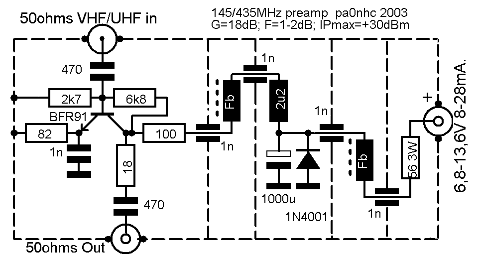
- solder the 1000pF feed through capacitors first.
- solder each of the four screening walls at one point onto the bottom of the box.
- solder them to two more places onto the box sides. See photo.
"Fb" are VHF ferrite beads.
Functional test :
When finished, check the current drawn, it should be 28 mA for best IMD performance.
You can correct it by changing the value of the emitter resistor of the BFR91.
Then check the voltage gain at 145MHz, it should be 18 dB.