| << |
A600 PA project :
Its problems and the solutions.
© The use, copy and
modification of all info on this site is only permitted for non-commercial
purposes,
and thereby explicitly mentioning my radio amateur call sign
"PA0NHC" as the original writer / designer / photographer /
publisher. Update
: 20211106. |
My original amplifier PCB V2 showed the
following problems ending in blown MRF300B FET :
| 1. |
A to low parallel
impedance was measured over balun T5 (possibly damaging Q2).
|
| 2 |
When switching-"ON" the
external 50Vdc supply, resistors R31/32 injected an up to +17V
DC-pulse onto the FET gates.
|
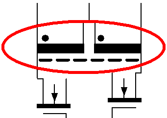
| 3 |
Q1/2 outputs were not forced to
balance, and chokes
L1 and L2 could show DC saturation.
|
| 4 |
The output of TR1 was floating, not
forced to balance.
|
| 5 |
The amplifier bandwidth was not limited to the used frequency range.
|
 After
eight modifications, my PA fulfils my expectations. Performance
is reliable,
After
eight modifications, my PA fulfils my expectations. Performance
is reliable,
as
long as
- drive power is max 1W, and
- not causing to high output power combined
with
- an LPF set to a wrong frequency band.
After a lot of E-mail traffic between ON9BOG and me, again testing and again
damaging another Q2, the below described modifications were developed. They resulted in (20210125)
:
- A robust amplifier.
- Less needed drive (1Wrms).
- Efficiency at 400W output : 56% (Power input 15A x 48V).
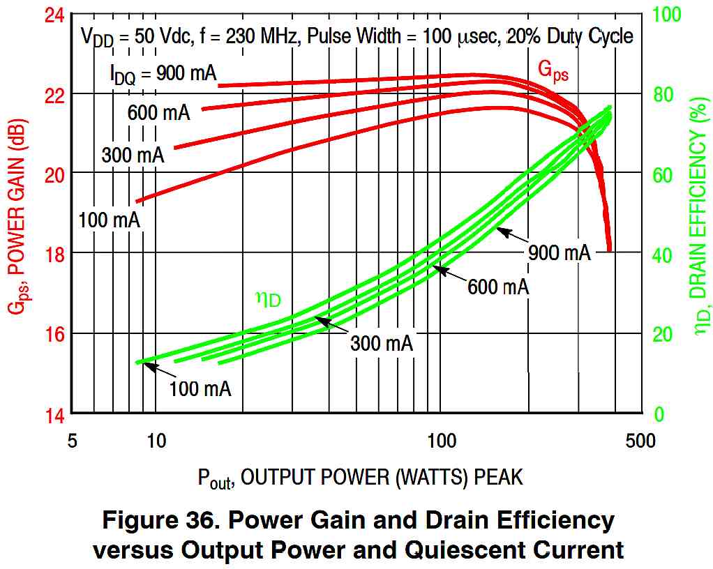
20211106 TIP1 (ON9BOG) : such FET
PAs deliver max. power to a 60 Ohms load, not to a 50 Ohms load.
TIP2 : the best amplifier linearity was
achieved (see NXP data in the graph) :
- By adjusting both FET gate bias
voltages for each FET Idq = 0.9 Adc,
- And by NOT driven to a distorted 600W output, but to
a clean
(and legal) 400W SSB output.
In practice, my pa delivers a clean 400W, and
maximal 450W, with drive of <=1W.
Modifications.
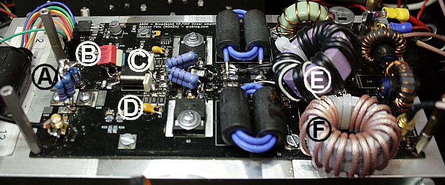
|
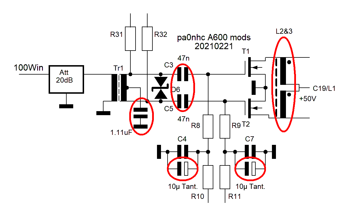
REM: see also modification F,
G and H.
|
|
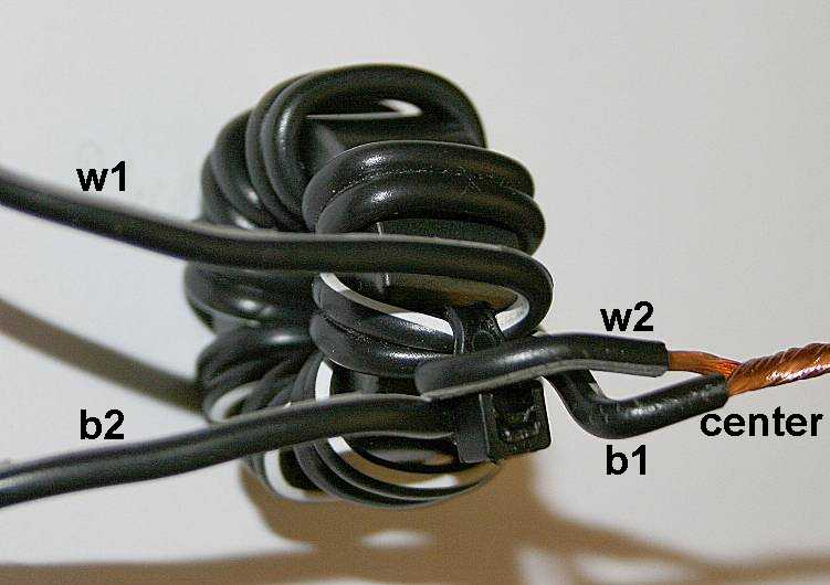
(b=black, w=white)
E1.
Ver. 20201018. 17.5 uH.
This balancing transformer is replacing L2 and L3.
Both winding halves are connected in series
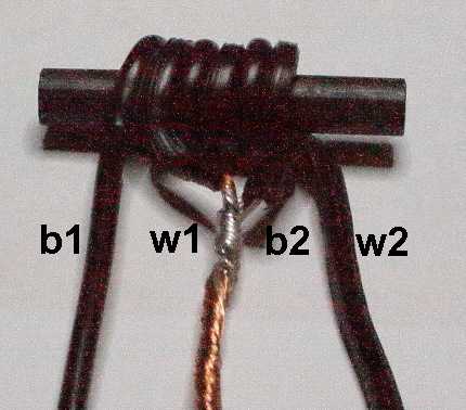
(b=black, w=white)
E2.
Even better transformer Ver.
20201217 : 1.72 uH.
See changes to C8 and C9.
This balancing transformer is replacing L2 and L3.
Both winding halves are connected in series
|
Modifications to prevent damages to Q1/2,
and to improve IMD and stability, in the order of importance.
Ver. 20210320 / 20211106..
| A.
|
20211106 :
- Using a Hermes Lite2 SDR TRX, and a 6dB attenuator (3x2dB 2W in series)
inserted between the back
panel PA input and the PA PCB input, you can drive
the PA fully to 450W output, with only 2.4W HL2 output,
resulting in 0.6W PA drive. Thereby protecting the PA against
damage due to to high drive power, and driving it with low VSWR
from 50 Ohms impedance.
- When using a 100W TRX and a 20dB
100W input attenuator, the drive power is also limited to a safe 1Wrms.,
and the driving TRX has best linearity.
|
|
F.
|
Improve output balance.
Replace balun (CMC) T5 by a better,
higher-Z Common Mode Choke.
Wind fourteen (14) turns RG316 on a 29mm #31
FairRite core 2631801202 .
|
|
D.
|
Prevent the injection of a strong DC pulse on Q1/2 gates when switching-on the 50V power
supply.
Connect 10uF 25V tantalum capacitors with minimal short
wires each in parallel to C4, and to C7.
|
|
C.
|
Replace C3 and C6
each by a 47nF 400V film capacitor.
|
| E2. |
Improve the output balance
by replacing chokes L1/2 by one balanced transformer
(TNX
to ON9BOG) :
- Wind 3 turns 6x2.8 mm (1.5mm2)
twin
speaker cord on a 8x50mm Ui=300 ferrite rod (Conrad orderNr. 1565952
). Total inductance about 1.72 uH.
===>>
Then tune this
transformer to about 7.5 MHz resonance as follows :
-
Solder at
Q1 between drain and source 330 pF MICA .
- Solder at Q2 between drain and
source 330 pF MICA . |
|
B.
|
Force
input transformer TR1 output to be in balance :
Connect the center of the secondary of T1 for RF to the PCB ground
plane.
- Connect 10n + 100n + 1uF film capacitors in parallel.
- Remove a little outer insulation at the
center of Tr1 coax screen.
- Connect this paralleled capacitor trio very shortly
between this center of T1 sec. and the nearby GND connection of T1 primary.
|
|
G.
|
Extra safety measures :
Limit the bandwith of Q1/2
to about 50MHz, thereby reducing the risk of RF instabilities (possible tendency to VHF
oscillations) as follows :
- Loosen the gate pins of both Q1
and Q2 from the PCB !!
Static precautions !!
- Solder a 3.3 ohms 0.25W metal film
resistor between Q1 gate and R8.
- Solder a 3.3 ohms 0.25W metal film
resistor between Q2 gate and R9.
|
| H. |
Hard limit the input power :
- Remove
the original D6 ( was +-12vpp).
- Solder a surge
diode CDSOD323-TO5SC (is now +-6Vpp) on its place at the connections of the secondary of Tr1.
|
|