|
|
| << |
The building process
of my A600 PA
and more details. |
This project is not a beginners project.
It demands knowledge and skills.
|
|
The subjects on this page :
- Metering.
- Wiring.
- Low pass filter assembling.
- Cooling, cooling profile, fans.
- Cabinet drilling and tapping.
- Grounding.
- Back panel.
- Used PCBs.
- Input attenuator adaptation.
- Drive indication.
- Construction photo's.
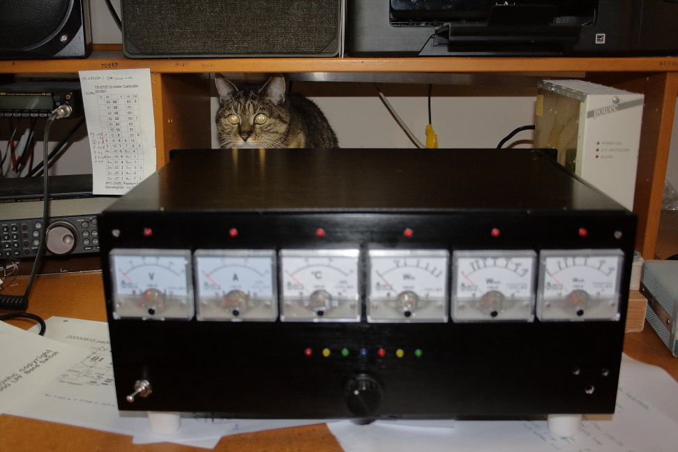
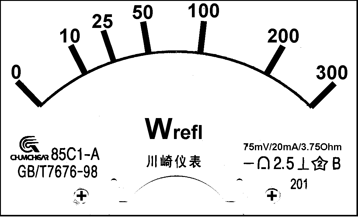
Metering.
These meter scales can be
printed and glued on de back side of the existing scales. |
|
|
As i do not want to read small characters on a small LCD screen for monitoring the amplifiers performance, i decided to use six small and cheap 1 mA 85C1 type moving coil meters (costs less than $30 at Aliexpress) to watch the six Power Amplifier PCB metering signals. These meters monitor DC signals coming from the 2x6 IDC J5 output bus on the amplifier PCB, and can accurately represent all signal levels measured at the PCB itself : Supply voltage, Supply current, Cooling temperature, FET gate drive voltage, Output power and Reflected power. The used J5 signal output lines at the PA PCB have different output levels and source impedances. Active buffer stages are thus needed to drive the lowZ 1mA 85C1 moving coil meters. The drive detector output impedance (pin J5-12), is very high. It is therefore loaded by R47 (22 kOhms) to prevent misreading and drift due to the leakage current of the buffer IC40 input. The drive meter indication should be adjusted after measuring the peak drive voltages at the FET gates, using a wideband oscilloscope.
In my prototype, six little PCBS are screwed onto the six 85C1 M3 meter connections. The input of each buffer has an RF filter, helping to make the metering system immune to RF fields inside the cabinet.
Each meter PCB contains a trim pot for adjustment of the meter FSD. The alarm level should also be adjustable. If an alarm threshold is passed by the input signal, a warning LED burns above that particular moving coil meter. These "Alarm LEDs" are fitting into 5mm holes into the front, above their respective moving coil meters, and are secured in place with contact glue. .
New PCB design, replacing all six single meter boards.

Updated new PEAK meter interface board.
This 222x54mm PCB could be mounted onto the cabinet floor in the vicinity of the moving coil meters. Its connections are easy and reliable made using 5mm pitch JST XH male PB busses and 20cm long female connection cables. Both ground surfaces of the metering PCB are FLOATING from its M3 mounting holes AND PA input. But these ground surfaces are connected to the "Minus" pin of the 12Vdc input bus. There is a possibility to connect these ground surfaces to the PApcb ground or CABINETground by installiing a jumper. In these cases, it is assumed that the minus 12Vdc pin is not connected to the metering PCB 12V power input, but to the PApcb ground or to the cabinet ground. It is not advised to use multiple groundings, to prevent ground loops.
At the left side is a 2x6 IDC bus for connection with a 12 wide flat cable and the same type bus "J5" at the PA unit PCB. At the right top the RF-filtered 12-20Vdc power input for all circuits. The regulator output is the 5Vdc reference voltage for the meter circuits. It is protected against input voltage short circuit, and wrong output polarity.
Each meter buffer circuit is identical and designed for use with a 1mA / 156 Ohm moving coil meter. Each buffer input is RF filtered and protected against input over voltage. The input of the "Drive" meter circuit (J5-12) is already shunted by 22 kOhms, to prevent meter deviations due to the infinitive detector source impedance, and the (uA) LM324 input leakage currents.
The updated metering circuits are peak detectors. The meters are therefore reacting fast, and declining slowly. Each meter circuit contains three precision resistor trimmers, for calibration of "Gain", "Full Scale Division" and "Alarm level". A jumper enables to connect the particular alarm output to a common "Buzzer" line. When the input signal passes the adjusted alarm level, the accompanying warning LED lights, and a buzzer can sound. Meters and accompanying warning LEDs are connected with JST XH male 5mm pitch PB busses, and 20cm long female connection cables.
Meter and alarm level calibration can be done by supplying a (for each meter different) DC voltage to the meter buffer input, according to the A600 J5 with the kit supplied signal level specifications.
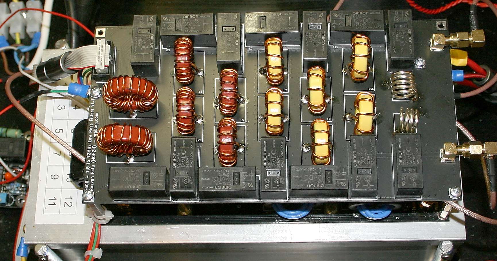
LPF
IMPORTANT : to prevent damage to already
installed relays when later soldering coils : FIRST place
and solder all coils, before doing relays.
|
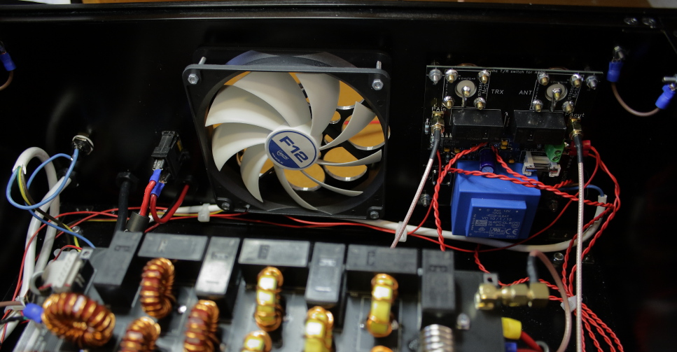
|
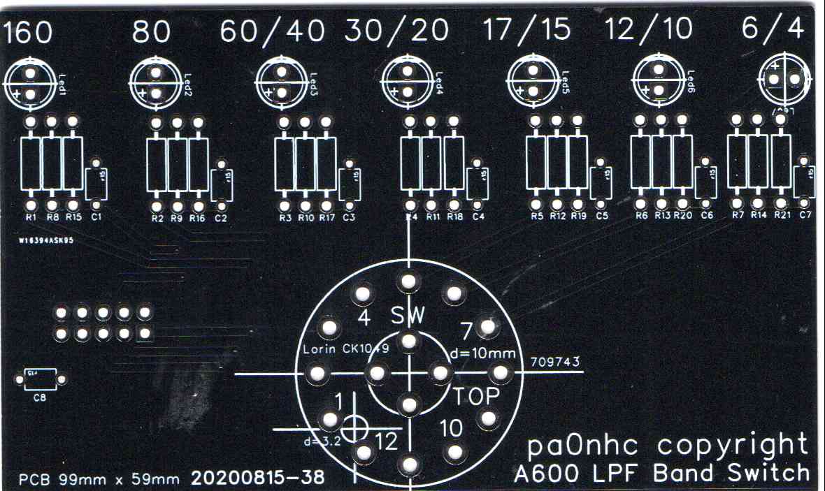
When the LPF kit from QRPBLOG.COM was delivered, all SMD components were already soldered. The LPF PCB will simply be installed on top of the PA unit. My LPF is switched by an at the front panel installed (by me developed) band switch PCB. Seven LEDs in the cabinet front indicate which filter is activated. Switching PCB, LEDs and LPF are powered by the 12Vdc supply from the T/R PCB.
The switching PCB supplies lowZ, and RF bypassed, TTL compatible, DC signals to the LPF PCB. They are connected by a 10 wide flat cable and 2x5 IDC connectors. To suppress induced RF currents, three sets of small #31 ferrite cores are installed over that flat cable.
Soldering the components on the LPF.
All supplied coil wires are INSULATED by lacquer, the silver plated wire
is lacquer insulated too.
After winding a coil, shorten the wire ends so they can protuede the PCB by 5mm..
Then carefully remove 1cm length of insulating lacquer from these coil ends, and carefully tin that wire
end.
A handy
tinning procedure is :
- Add some extra solder flux to both
wire end and
solder iron tip (this makes tinning much easier).
- Adjust the temperature of a thick solder iron tip to 420 C (four
hundred twenty degrees Celsius).
- Add fresh tin to the solder tip.
- Heath the wire by holding the tip against the exposed bare copper point of the wire.
- After a short while, the lacquer starts to bubble.
- Then immediately add fresh tin-solder
and at the same time
- Move both tip and solder slowly over the wire end until enough wire length is tinned.
- Let the wire cool down.
- Using a knife, remove ALL debris.
Be sure the whole surface of the wire end is tinned and no lacquer
remains.
Cooling.
|
|
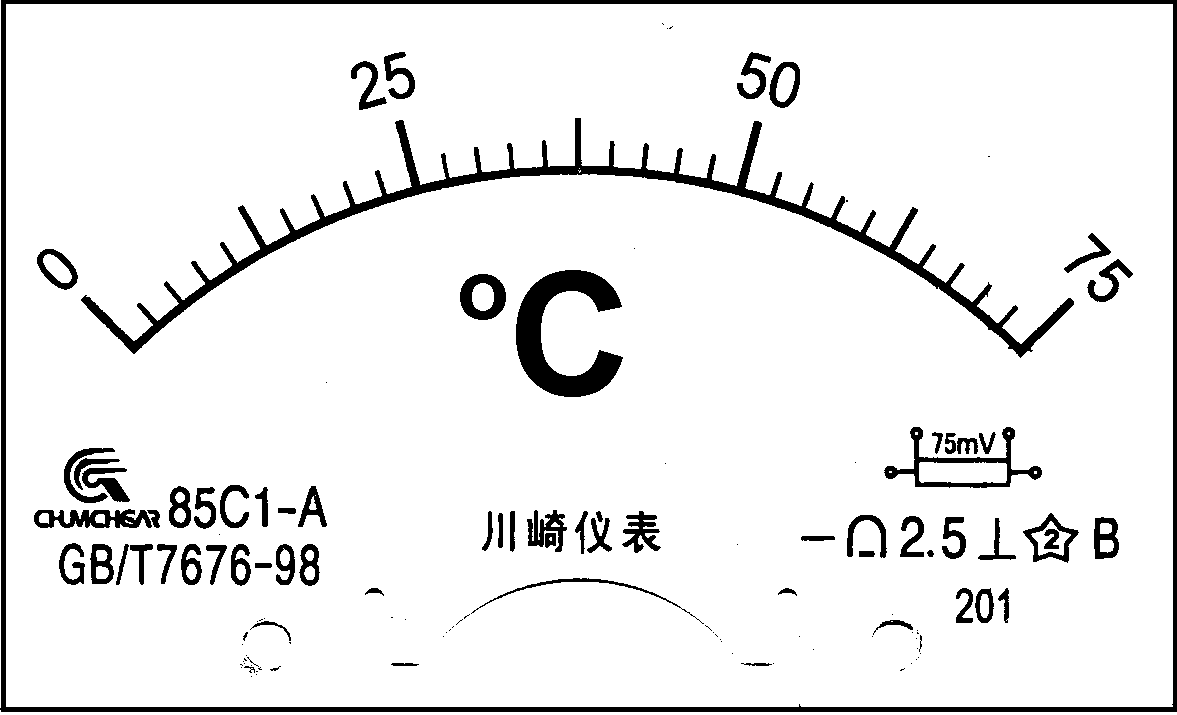
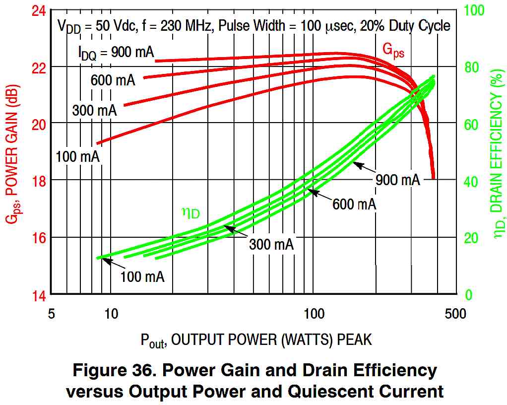
It is difficult to measure the MRF300 FLANGE temperature. The temperature of the plastic MRF300 bodies (having the at least same temperature as their cooling flanges ?) showed to have an up to 6 C higher temperature than the cooling profile near the FETs flanges. According to NXP, the max. flange temperature for an MRF300 is 74 C @ 8 A drain current.
My maximal allowable heath sink temperature at 16A x 48Vdc supplied power is therefore calculated to about 68 C.
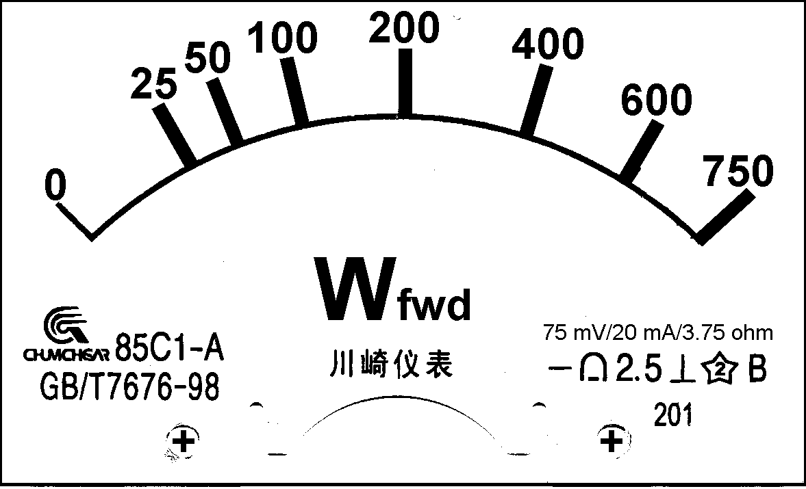
Loaded with my loop antenna and 400W carrier, the consumed
power is 16A x 48V, the max specified by NXP.
Max. output power for low distortion SSB is 400W. See bias curves.
Giving more drive power, the amplifier
proved to be able to give nearly 600W output into a 60 Ohms dummy load.
But I do advise NOT to push to the max power of 600W. It results
in IMD (SSB splatter and CW clicks) and is not contributing to amplifier
lifespan. That is my reason to use a 100W/20dB input attenuator, it limits the
max output when driving the PA with a 100W TRX.
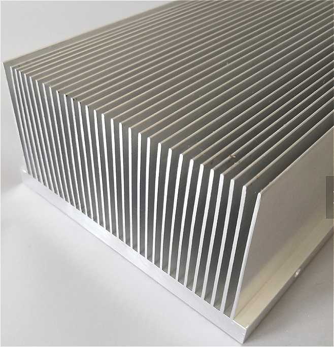
I use an
oversized ALU cooling block. =>
This prevents buying an extra and expensive 10cm wide, 20cm long and 12mm thick, pure copper heath
spreader, and difficult drilling and tapping of a lot of holes.
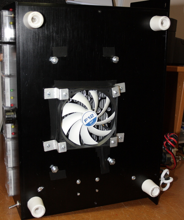
For best cooling, i use two Arctic F12CTY fans. They regulate th aistem automatically measuring the cooling block temperature with sensors. The first fan is installed under the cabinet bottom, blowing cool air directly into the fins of the cooling profile, right under the position of the power FETs. The second fan at the back panel removes warm air from the inside of the cabinet. The practical thermal resistance of the cooling block proved to be a little better than 0.1K/W Long SSB QSO's with moderate compression proved to be no problem.
Cabinet, drilling and tapping.
As the
cooling block is 8cm high, and the PA PCB, and the LPF on top of the PA are
both 4cm high, they demanded for an at least 17 cm high cabinet.
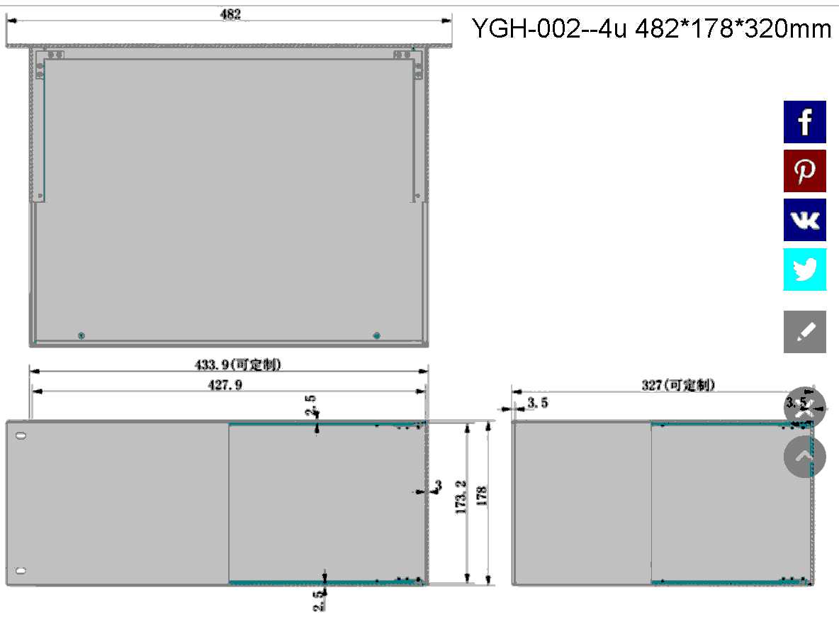
At Alibaba i found a 4 units high 19" cabinet kit. Consisting of six 3mm thick die cast, milled and drilled, black anodized ALU panels. These panels must be screwed together with small 3mm black flat head screws, and corner connections. All fitted perfectly.
|
Search for 19 inch 4u 482*178*320mm 19 inch server rack aluminum amplifier chassis. |
Warning : the anodization of the panels create black INSULATING layers onto the bare aluminum. Screwing them together does NOT connect them electrically.
|
|
|
|
All grounding holes in the cabinet should be tapped, for the best
electrical contact between panel and screw.
A lot of holes must be drilled.
Do not drill indoors, to keep the XYL
friendly. Or the house will be infested with aluminum debris.
Use new, sharp drills, and cool the drills
with alcohol or lubricate with oil. Use slow rotation.
Tapping of holes can best be done using single machine taps, while
lubricating with oil. Regularly stop.
After a half to two turns, turn 1/2 turn back to
break the curl loose.
If to much force must be used, remove the tap and its debris.
After finishing a hole, CLEAN the tap fully from debris.
The 50mm holes for the 28C1 type 1mA moving coil meters, MUST be drilled using a drill stand, and
a multi-tooth 50mm high speed steel drill.
Use a piece of flat wood to support the ALU plate, and screw them temporarily together.
Then pre-drill the big holes first using a 6mm drill, to be sure of the exact
hole position.
Drill with slowest speed, and use
the correct pressure to prevent blocking of the drill.
While drilling, keep
lubricating to reduce drag and heath.
Remove aluminum curls and debris regularly.
Grounding
problems.
As all cabinet panels are nicely black anodized, they are therefore INSULATED from each
other. I interconnected all panels with short wires, and then at one point to
the central grounding point at the cabinet bottom plate.
One point at the cabinet bottom plate serves as
central grounding point
for :
- the mains ground safety wire,
- all side panels (with one wire),
- the cooling profile with PA PCB and the LPF PCB with one wire,
- the - 12Vdc of all meter buffer stages.
Drill
ALL grounding holes (the back panel too) with 2.5mm, and tap them with M3.
Use tooth rings under these screws
and nuts, which penetrate the insulating layer. MEASURE groundings !
The back panel.
The 240 Vac mains input is fused by a 5mm x 20mm 5A slow
blow fuse.
The external 50Vdc power supply is connected to this 240V~ mains output by
means of an Euro power cord with female plug.
The 50Vdc power supply output is connected with a high current DC connector pair, and
at the PA-back panel fused by a 25A automotive fuse.
As that external 50Vdc power supply needs some convection cooling, i placed it
on two wooden feet, creating breathing space under its bottom.
|
|
|
I decided to design my own T/R switching "BackPanel" PCB, as i do not need an Elecraft KPA1500 interfacing, nor a second antenna connection.
My back panel PCB performs T/R switching, and two LEDS at the
cabinet front indicate "Receive / Transmit" modes.
To switch the PA between standby and amplifying the RF drive power, a sequenced
relay output from the driving TRX must be connected to the back panel BNC
"Key" bus.
This TRX relay output must first send the switching command to the PA, before
actually starting to transmit.
When stopping transmitting, the TRX relay output should wait a moment, before
removing the switching command to the PA.
To prevent RF stray currents through the bottom plate, the SMA and N connectors on the T/R PCB are electrically FLOATING, and only connected to the PA PCB via their SMA cables.
The T/R PCB is mounted with some free space between PCB and back panel, resulting in the N connectors and BNC connector not making contact with the cabinet back panel. Use distance bushes, or a few rings or nuts as spacers between the PCB and the back panel.
During
receiving mode, the PA bias current is reduced to zero by the T/R PCB "Inhibit"
output, reducing heath and power consumption.
A toggle switch at the front of the PA can cut this input, to force the PA to
"standby".
The FANs keep running then, but the PA cannot be
activated to amplify incoming RF.
The metering- and the FAN switching circuits are designed for 10-20Vdc supply voltage, making a stabilized supply unnecessary.
My back panel also contains an unregulated 12V/10W DC power supply, which feeds the metering circuits, the band switch circuit, the FAN regulator and the FANs. Its output is protected with a 1A 5x20 mm fuse. The minus of the 12V power supply output at this PCB however is directly connected to the cabinet back panel (and to all cabinet parts, and to the bottom plate central grounding point).
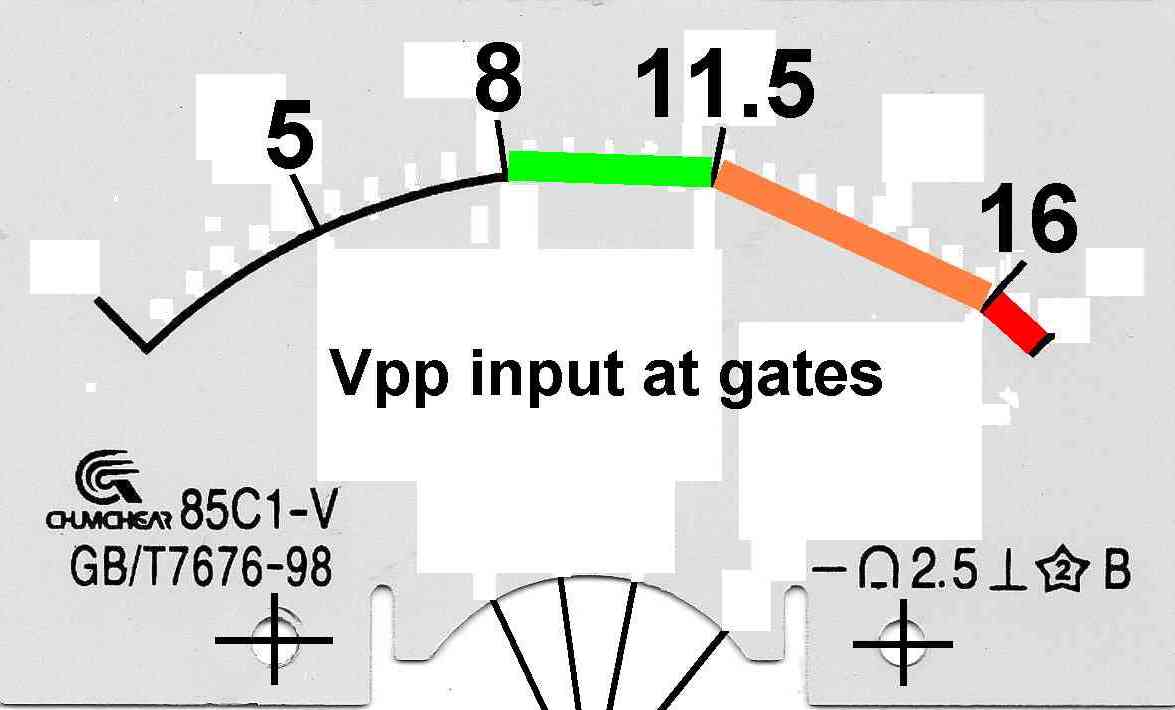
The important Fet-gates drive indication.
The drive peak meter indication should be adjusted according to measured
RF drive voltages.
The output of the RF drive "power" detector is a voltage
from a very high impedance source.
This voltage is measured
at the input side of the
input matching transformer T1.
The FET gates are driven by VOLTAGES, not currents nor power.
According to NXP, the
max allowable gate peak voltages in respect to the sources are +10V / -6V.
Higher voltages will damage
the FETs.
As not the amplifier input power, but gate-RF-drive voltage
is critical, the RFinput meter should indicate PA input RF-peak-to-peak
VOLTAGE.
The drive voltage at the gates was measured with an Tektronix
465B 200 MHz oscilloscope, and was nearly 7Vpp when driven with 100W, generating
600W output. With modification "B" at the secondary of T1, both drive
voltages on gates Q1 and Q2 showed to be exactly the same pp value and wave
form.
For 400W output about 5Vpp drive was needed. Changing D6 for a 10Vpp
bipolar surge arrestor diode can help preventing damages to the FETs.
Bias setting.
Razvan advises a Q1 and Q2 idle current of each 0.2 Adc. But with this bias setting the linearity of the PA will not be optimal. Small drive signals will not be amplified. Such a small idle current acts a signal threshold, distorting the signal. The effect is like a compander. It is only tolerable for CW modes (CW, FM, digital)..
 According to NXP data
an idle current of 0.9Adc for each FET) gives the best linearity.
According to NXP data
an idle current of 0.9Adc for each FET) gives the best linearity.
As in the given gate bias circuit the maximal idle current is 0.8 A, i adjusted each
FET idle current both to 0.8Adc.
With inhibited bias, the PA PCB still draws about 20mA.
When Pure Signal mode is used, the bias
can indeed be set to 2x 0.2A. The then in the PA generated distortion is neutralized by the strong negative feed back from the Pure Signal software.
The
heath-production is then reduced by 1.4 x 50 = 90W, still with very low IMD
levels. NICE.
Idle current adjustment (no pure
signal) :
First turn both bias trimmers fully ant-clock wise. PA current is then about
20mA.
Then adjust Q1 for 0.9A more DC current (to totally 0.92 A).
Secondly adjust Q2 for 0.9A more DC current (to totally 1.82 A).
Second harmonic suppression.
As the MRF300AN and MRF300BN are not a set of paired semiconductors (not having exact equal properties), best 2nd harmonic suppression
could be achieved by adjusting at 3.55 MHz one of the two FET idle currents,
until the second harmonic at 7.1 MHz has minimal value.
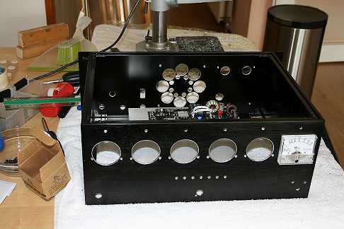
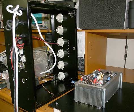
Construction photos :
Back-panel inside.
At the left side : 240V~/5A mains power fuse and 50V/25Adc fuse.
At the right : The T/R switching PCB with 12V / 0.8 Adc power supply for the
meters, FAN and LPF.
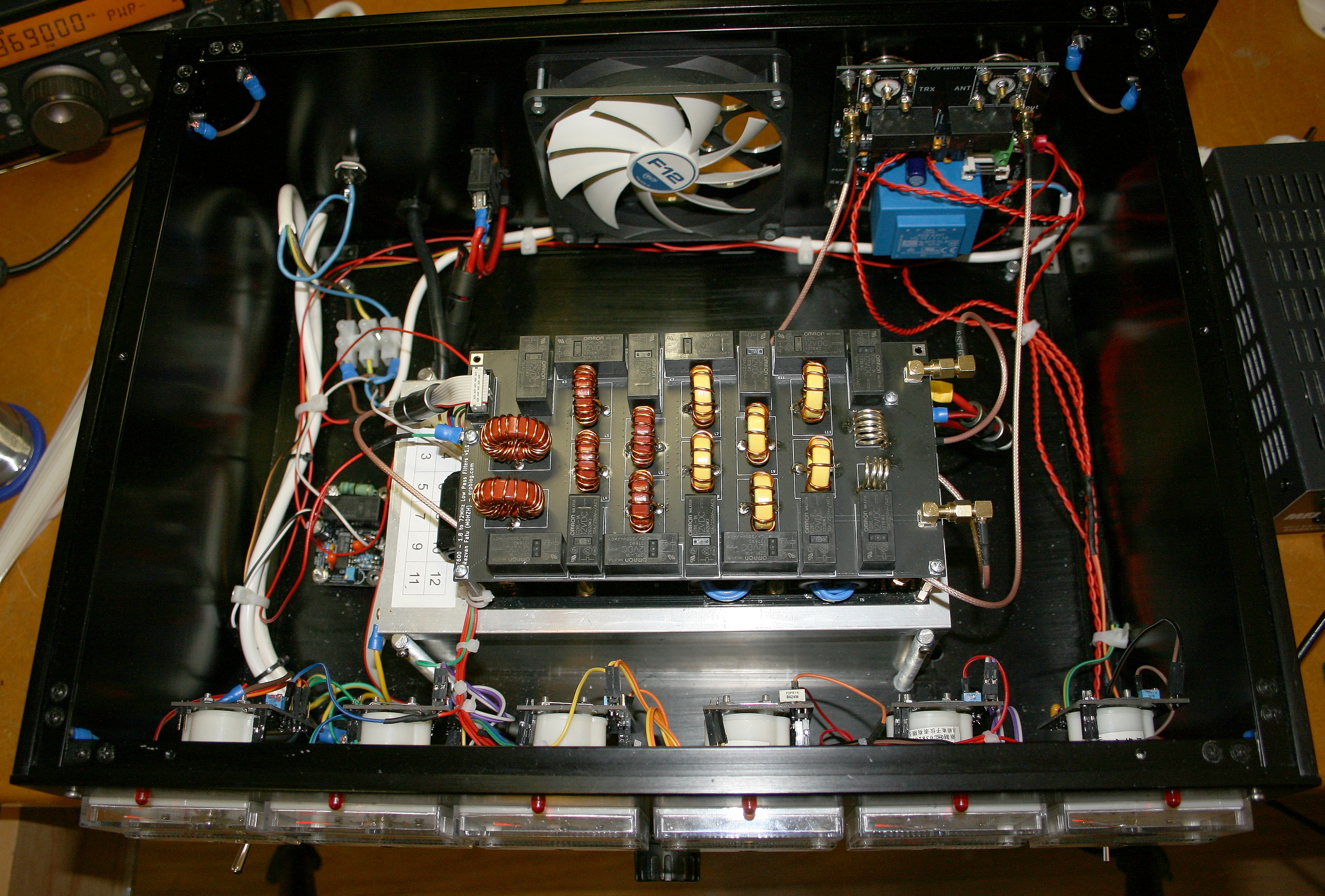
Wiring overview.
At
the left on the bottom the old FAN regulator PCB. It is removed after installing
the Arctic F12TC
Temperature Controlled fans.
|
|
At the left:
the N busses for antenna and TRX, with below them the
BNC bus for connection of the T/R signal from the ACC bus at the TRX.
Holes for the N-busses and the BNC bus are drilled big enough to enable plugs to pass the panel. They
are
INSULATED from the back panel to prevent stray RF currents. All bigger holes are drilled using a step-tapered drill. A drilling
template is available. The four M3 grounding holes should be drilled 2.5mm and tapped M3 for good ground
contact. Small size door-buffers are used as feet.
At the right :
A 50V / 25A automotive fuse for the 50Vdc input, and a 5A fuse for the 240V~
mains in/output.
Below are the 50Vdc cable, the 240V~output to the power supply, and the 240V~ input
from the mains power.
The three Commom Mode Chokes chokes use 29mm #31 cores. FairRite "SnapIt" #31 cores with a 19mm
or wider hole are also useable.
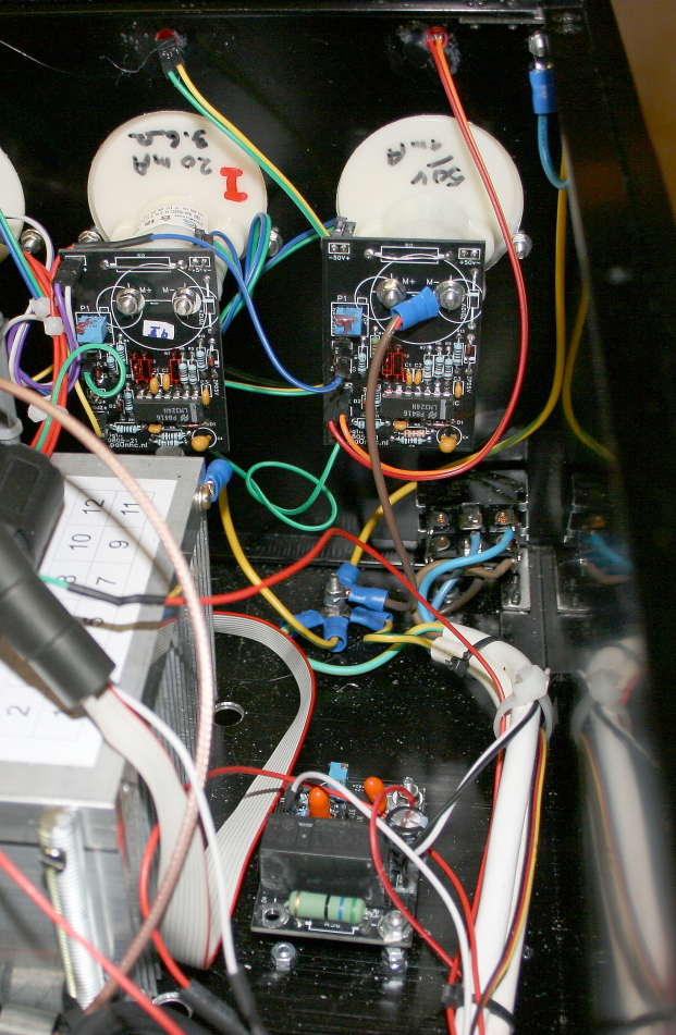
The blue wire at the top connects the cabinet side panel to the cabinet front panel. It is via the yellow/green wire connected to the central grounding point at the cabinet bottom plate. At the bottom a long M3 screw which functions as central ground point. The brown wire is the -12V grounding wire for all meter circuits. The meter PCBs are mounted directly onto the meter connection bolts. Also at the bottom the now removed FAN regulator PCB. |
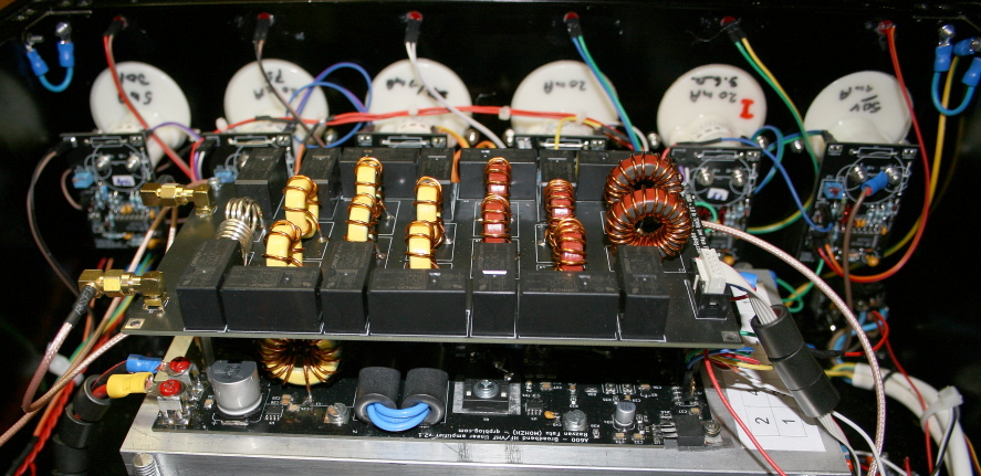
On top of the PA-PCB, the LPF PCB. A 10-pole flat cable connects the band
switch at the front panel (not shown) with the LPF-PCB
on top of the PA unit. |