 -- -- |
 |
| << |
A600 PA back panel
board. 20210407. |
. . . to be sure to get the latest page updates from the SERVER .
| -- |
|
Click-right on a picture to download it.
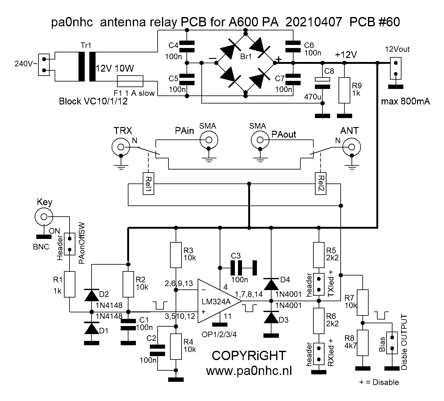
As i do not need (cannot use) an Elecraft KPA1500 interfacing, nor need a second antenna connection, like available on the QRPblog PCB, I decided to design my own T/R switching "Back Panel" board.
My back panel board performs T/R switching. Two LEDS at the cabinet front indicate "Receive / Transmit" modes. In order to switch the PA between "standby" and "amplify", the connected transmitter must deliver a sequenced "Key" ("PTT") signal to the BNC "Key" bus at the PA back panel board. Sequenced means, that this "Key" signal must first switch the PA to "On", before actually starting to transmit. When stopping transmitting, the "Key" signal should wait a moment before switching the PA to "Standby". Delays of 10mS proved to be adequate.
The (automatic to temperature changes responding) fans, and metering circuits, are designed for 10-18Vdc supply voltage, making a simple non-stabilized power supply possible. My back panel board contains a simple, unregulated 12V/10W DC power supply. It feeds the metering circuits, the band switch circuit, the LPF and the FANs. Its output is protected with a 1A fuse.
REM : The "Minus" of the 12V power supply output is connected to the back panel board "Ground", and is by two mounting screws connected to the cabinet back panel. As all cabinet panels are positively interconnected by wires, the bottom plate central grounding point, the PA cooling profile and the PA board are all connected to -12V.
The LPF board is with one wire connected to the PA board ground near J5, and with one wire connected to the back panel +12V output.
The ground surfaces of the LPF switching board at the cabinet front are electrically floating. The power of this LPF switching board is connected by a 12 wide flat connecting cable (besides to signals) to the +- 12Vdc of J5 on the PA board.
Construction details.
To prevent RF stray currents running through the cabinet back panel and bottom plates :
The
SMA-type "PAin", "PAout", and N-type "TRX" and
"Ant" busses on the T/R back panel PCB are electrically
FLOATING from the PCB "Ground" and
the cabinet back panel "Ground".
Only the "PAin" and "PAout" SMA cable screens connect the back penal pcb
to the "ground" surfaces at the PApcb and LPFpcb.
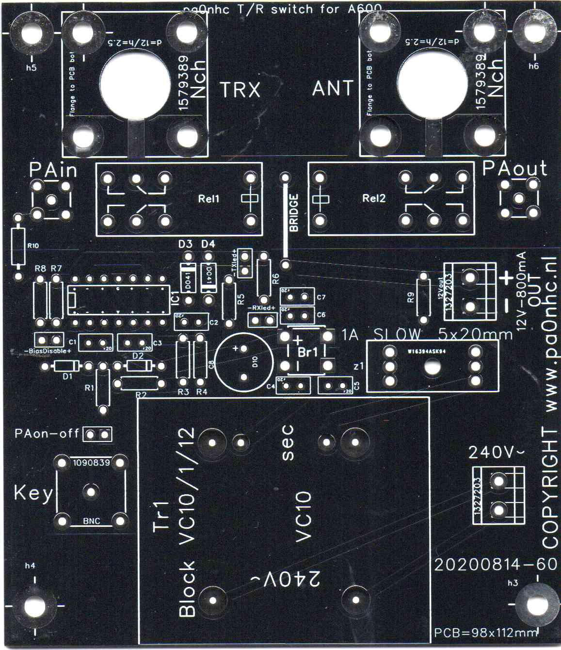
The back panel PCB "TRX", "ANT" and "Key" connectors are positioned onto the bottom side of the back panel PCB. The back panel PCB is mounted with some free space between the board and the back panel. You therefore have to use distance bushes, or a few rings or nuts as spacers between the PCB, and the inside of the back panel. The N-connectors and BNC connector may not making direct contact with the cabinet back panel.
A "STBY" toggle switch at the front of the PA can cut the "Key" input, to force the PA to continues be "standby". The PA can then not be activated to amplify incoming RF.
During receiving and standby mode, the PA bias current is reduced to zero by the T/R PCB "Inhibit" output on the backpanel PCB. Thus reducing heath generation and power consumption. The Back Panel board "PAon-off" IDC pin must be connected to the PA board "Inhibbit" pin to accomplish this.
Installing components.
Pay attention to the polarity of diodes (stripe on the diode body = cathode.
PCB marked "k". Anode is PCB marked "a").
Pay attention to the position of the notch in the IC socket and the notch or dot
(= pin1) on the IC.
Pay attention to the polarity of electrolytic capacitors. The longest wire
is + (positive).
Place and solder components in the following
order :
- Solder the "TRX", "ANT" and "Key" busses
with their flanges to the PCB BOTTOM side.
Solder their pins at the PCB TOP side.
- Place all other components at the PCB TOP side, and solder them on the
PCB BOTTOM side.
- "Bridge" wire, BR1, IC socket, 2pin
IDC bus, "PAin", "PAout", 240V connector,
12V connector, Fuse holder, elco, and
all other capacitors, diodes and resistors.
- Solder the the transformer and the relays as last ( !! plastic relay cases are
sensitive to deformation by heath, then blocking relay action !! ).
CHECK if all components are correctly placed and soldered well.
Back panel partslist 20210407
Download
PDF partslist.
A few parts can be ordered at Conrad.nl , to be sure to fit the PCB.
| Part reference | Value | Total | Conrad.nl Order Nr. |
| R1,9 | 1k | 2 | |
| R2,3,4,7 | 10k | 4 | |
| R5,6 | 2k2 | 2 | |
| R8 | 4k7 | 6 | |
| C1,2,3,4,5,6,7 | 100n 50V ceramic RM2.5 | 7 | |
| C8 | Elco 470uF 35V D=10mm RM5. | 1 | |
| D1,2 | 1N4148 | 2 | |
| D3,4 | 1N4001 | 2 | |
| BR1 | DIL bridge rectifier B40D. | 1 | |
| OP | LM324A |
1 |
|
| 14 pin IC socket | 1 | ||
| TRX, ANT | Female N-bus, flange, panel mount. Solderable. |
1 | |
| PAin, PAout | Female SMA-bus, flange, PCB mount. Solderable. |
1 | |
| Key | Female BNC-bus, flange, PCB mount. Solderable. |
2 | 1090839 |
| PAonoff, 12Vout, Disable | 2 pin male header RM2.5. | 3 | |
| F1 | Fuse holder 5x20mm | 1 | 532908 |
| Fuse 5x20mm 1A slow blow. | 1 | ||
| TR1 | Transformer 230V~ / 12V~ / 10VA Block VC10/1/12 |
1 | 710458 |
| Rel1,2 | OMRON G2RL-2 DPDT relais 12V | 2 | 503903 |
| 240V~, 12V~ out | 2 pole screw block RM5 | 2 | 1327203 |